
How to program stm8s with arduino and stm8flash
stm8s-programmer-arduino
Guidelines to compile and upload program to stm8s
Setup
- Install arduino board: https://tenbaht.github.io/sduino/
- Install flash tool: https://github.com/vdudouyt/stm8flash
Tool: ST-LINK V2 (don’t forget updating udev rules, check here
Before flashing, must connect either ST-Link V2 and USB Cable. In arduino IDE: programmer: ST-Link-V2 board: stm8s103f3
In order to remove writting protection:
echo "00 00 ff 00 ff 00 ff 00 ff 00 ff" | xxd -r -p > factory_defaults.bin
stm8flash -c stlinkv2 -p stm8s103?3 -s opt -w factory_defaults.bin
In arduino IDE:
- programmer: ST-Link-V2
- board: stm8s103f3
Thanks to @tenbaht for sduino reference. In order to get more detailed information, access https://tenbaht.github.io/sduino/
Generic STM8S103 breakout board
These simple breakout boards are available on aliexpress for well under one Dollar (I got mine for 67 cent each, including shipping from China). These boards are my main development platform.
They are very similar to the ESP14 Wifi-boards and most programs will work fine on those chinese gems as well.
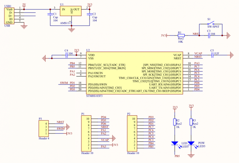
The STM8S103 breakout boards are build around a CPU STM8S103F3P6 with 16MHz internal oscillator, 8kB flash, 1kB RAM, and 640 byte EEPROM. The CPU includes a UART, SPI, I2C, PWM, 10 bit ADC, 3 timer, and up to 14 I/O pins - quite similar to an Atmel ATmega8.
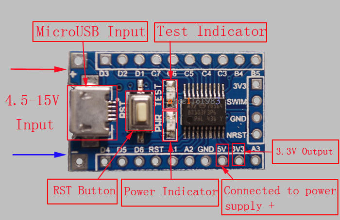
One (red) LED is connected to GPIO PB5 (CPU pin 11). This LED is low active. Please keep in mind that this is one of the I2C signals and using the LED blocks the I2C bus. The push button is for reset. The CPU runs on 3.3V, a linear regulator is integrated on the board. The micro USB connector is only for (5V) power supply, the data lines are not connected.
All CPU pins are easily accessible on (optional) pin headers (pitch 2.54mm, perfect for breadboards).
Unlocking a write protected MCU
My breakout boards came preprogrammed with a blink program and with active write protection bits. For unlocking before first use:
stm8flash -cstlinkv2 -pstm8s103?3 -u
Connection to the flash tool
I am using the ST-Link V2 compatible flash tool in the green plastic housing. The one in the metal housing uses a different pinout.
Connection to the flashtool:
| Signal name | P3 on CPU board | Green flash tool | Metal flash tool |
|---|---|---|---|
| 3V3 | 1 | 2 | 7 |
| SWIM | 2 | 5 | 5 |
| GND | 3 | 7 | 3 |
| NRST | 4 | 9 | 1 |
Pin number mappings
The Arduino environment uses its own pin numbering scheme independent from the physical CPU pin numbers. Many Arduino sketches and libraries contain hard-coded assumptions about the number of pins with special functions. Ideally, all these numbers would be the same and all programs could be compiled without changes.
In the end I chose a simple geometric numbering for the square UFQFPN20 package starting with port pin PA1 and counting up from 0. This results in this mapping:
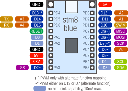
| sduino pin | STM8S103 CPU port pin |
|---|---|
| 0-2 | PA1-PA3 (PA1 and PA2 only weak output drivers) |
| 3-4 | PB5-PB4 (reverse order) |
| 5-9 | PC3-PC7 |
| 10-15 | PD1-PD6 |
- serial: 14,15
- SPI: 2,7,8,9
- I2C: 3,4 (true open drain. can’t drive a high signal without an external pull-up resistor)
- Analog: 6,11,12,14,15
- PWM: 2,5,6,12 plus either only 13 or 7-9 but not 13 (via alternate mapping)
pros of this approach:
- Easy and logical for use on a breadboard
- Very clear and logical port pin ordering
- TX and RX would be the rarely used analog pin numbers A3/A4 at the end of the analog pin number list
- At least the analog pins are in data sheet order
cons of this approach:
- Analog pins are still scattered around
- All functions use totally different pin numbers than Arduino
I am still not really happy with this mapping. Instead of simplifing things
it only adds another layer of abstraction and confusion. To avoid this I
added definitions for the regular CPU pin names like PA1 and PD2. In the
end, this notation seems to be a lot easier to me. I am open for suggestions
for a better pin number mapping.
The chosen pin mapping for the STM8S103 (possible alternate function in paratheses):
| Phys. STM8 pin | Name | Functions | Geometrical mapping | special funcion |
|---|---|---|---|---|
| 1 | PD4 | UART_CLK/T2-1/beep | 13 | PWM |
| 2 | PD5 | TX/Ain5 | 14 | Analog A3 |
| 3 | PD6 | RX/Ain6 | 15 | Analog A4 |
| 5 | PA1 | (OscIn, no HS) | 0 | |
| 6 | PA2 | (OscIn, no HS) | 1 | |
| 10 | PA3 | SS/T2-3 | 2 | PWM |
| 11 | PB5 | SDA LED | 3 | |
| 12 | PB4 | SCL | 4 | |
| 13 | PC3 | T1-3/[T1-n1] | 5 | PWM, (n~) |
| 14 | PC4 | T1-4/Ain2/[T1-n2] | 6 | PWM, Analog A0, (n~) |
| 15 | PC5 | SCK/[T2-1] | 7 | (~) |
| 16 | PC6 | MOSI/[T1-1] | 8 | (~) |
| 17 | PC7 | MISO/[T1-2] | 9 | (~) |
| 18 | PD1 | (SWIM) | 10 | |
| 19 | PD2 | Ain3/[T2-3] | 11 | Analog A1, (~~) |
| 20 | PD3 | Ain4/T2-2 | 12 | PWM, Analog A2 |
Special pins
The pins D3/D4 (SDA/SCL, PB5/PB4) are different from the others as they are true open drain pins. That means, they only can drive the output low or open. To drive it high, they require an external pull-up resistor. This is the reason why the LED on this breakout board is connected between +3.3V and the pins and not between the pin and GND as usual. This way it is possible to drive the LED by writing a zero to the output register.
D5/D6 (PA1/PA2, OscIn/OscOut) are weaker than the other pins. Try avoiding these pins for LEDs and other higher current applications.